- 您现在的位置:买卖IC网 > Sheet目录313 > AT27LV520-90XI (Atmel)IC OTP 512KBIT 90NS 20TSSOP
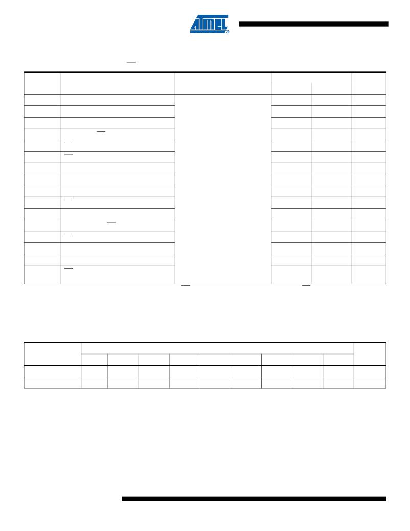
16. AC Programming Characteristics
T A = 25 ± 5 ° C, V CC = 6.5 ± 0.25V, OE/V PP = 13.0 ± 0.25V
Limits
Symbol
t ALE
t LAS
t LAH
t LP
t OES
t OEH
t DS
t DH
t PW
t VR
t VCS
t OE
Parameter (1)
Address Latch Enable Width
Latched Address Setup Time
Latched Address Hold Time
ALE Low to OE/V PP High Voltage Delay
OE/V PP Setup Time
OE/V PP Hold Time
Data Setup Time
Data Hold Time
ALE Program Pulse Width (2)
OE/V PP Recovery Time
V CC Setup Time
Data Valid from OE/V PP
Test Conditions
Input Rise and Fall Times:
(10% to 90%) 20 ns
Input Pulse Levels:
0.45V to 2.4V
Input Timing Reference Level:
0.8V to 2.0V
Output Timing Reference Level:
Min
500
100
100
2
2
2
2
2
47.5
2
2
Max
52.5
150
Units
ns
ns
ns
μs
μs
μs
μs
μs
μs
μs
μs
ns
t DFP
OE/V PP High to Output Float Delay
(3)
0.8V to 2.0V
0
130
ns
t AS
t AH
t PRT
Address Setup Time
Address Hold Time
OE/V PP Pulse Rise Time During
Programming
2
0
50
μs
μs
ns
Notes:
1. V CC must be applied simultaneously or before OE/V PP and removed simultaneously or after OE/V PP .
2. Program Pulse width tolerance is 50 μsec ± 5%.
3. This parameter is only sampled and is not 100% tested. Output Float is defined as the point where data is no longer driven –
see timing diagram.
17. Atmel’s AT27LV520 Integrated Product Identification Code
Pins
Hex
Codes
Manufacturer
Device Type
A8
0
1
AD7
0
1
AD6
0
0
AD5
0
0
AD4
1
1
AD3
1
1
AD2
1
1
AD1
1
0
AD0
0
1
Data
1E
9D
Note:
8
1. The AT27LV520 has the same product identification code as the AT27C520. Both are programming compatible.
AT27LV520
0911G–EPROM–8/07
发布紧急采购,3分钟左右您将得到回复。
相关PDF资料
AT28BV256-20SU
IC EEPROM 256KBIT 200NS 28SOIC
AT28BV64-30TI
IC EEPROM 64KBIT 300NS 28TSOP
AT28C010E-20TI
IC EEPROM 1MBIT 200NS 32TSOP
AT28C16E-15SC
IC EEPROM 16KBIT 150NS 24SOIC
AT28C17E-15SI
IC EEPROM 16KBIT 150NS 28SOIC
AT28C256E-15TI
IC EEPROM 256KBIT 150NS 28TSOP
AT28C64B-15SU
IC EEPROM 64KBIT 150NS 28SOIC
AT28C64E-25TI
IC EEPROM 64KBIT 250NS 28TSOP
相关代理商/技术参数
AT27LV520-90XU
功能描述:可擦除可编程ROM 512Kb (64Kx8) OTP 3V 90ns RoHS:否 制造商:Maxim Integrated 类型: 存储容量:1024 bit 组织:1 K x 1 接口类型: 工作电流:5 uA 编程电压: 工作电源电压:2.8 V to 6 V 最大工作温度:+ 85 C 安装风格:Through Hole 封装 / 箱体:TO-92
AT-28.63636MAGE-T
功能描述:晶体 28.63636MHz 30ppm 12pF -40 to 85C RoHS:否 制造商:AVX 频率:26 MHz 容差: 频率稳定性:50 PPM 负载电容:8 pF 端接类型:SMD/SMT 封装 / 箱体:1210 (3225 metric) 工作温度范围:- 40 C to + 150 C 尺寸:2.5 mm W x 3.2 mm L x 0.85 mm H 封装:Reel
AT-28.63636MAGK-T
功能描述:28.63636MHz ±30ppm 晶体 20pF 50 欧姆 -40°C ~ 85°C AEC-Q200 表面贴装 HC49/US 制造商:txc corporation 系列:AT 包装:带卷(TR) 零件状态:有效 类型:MHz 晶体 频率:28.63636MHz 频率稳定度:±50ppm 频率容差:±30ppm 负载电容:20pF ESR(等效串联电阻):50 欧姆 工作模式:基谐 工作温度:-40°C ~ 85°C 等级:AEC-Q200 安装类型:表面贴装 封装/外壳:HC49/US 大小/尺寸:0.449" 长 x 0.189" 宽(11.40mm x 4.80mm) 高度:0.161"(4.10mm) 标准包装:1,000
AT-28.63636MAHE-T
功能描述:28.63636MHz ±30ppm 晶体 12pF 50 欧姆 -40°C ~ 85°C AEC-Q200 表面贴装 HC49/US 制造商:txc corporation 系列:AT 包装:带卷(TR) 零件状态:有效 类型:MHz 晶体 频率:28.63636MHz 频率稳定度:±30ppm 频率容差:±30ppm 负载电容:12pF ESR(等效串联电阻):50 欧姆 工作模式:基谐 工作温度:-40°C ~ 85°C 等级:AEC-Q200 安装类型:表面贴装 封装/外壳:HC49/US 大小/尺寸:0.449" 长 x 0.189" 宽(11.40mm x 4.80mm) 高度:0.161"(4.10mm) 标准包装:1,000
AT-28.63636MAHI-T
功能描述:28.63636MHz ±30ppm 晶体 16pF 50 欧姆 -40°C ~ 85°C AEC-Q200 表面贴装 HC49/US 制造商:txc corporation 系列:AT 包装:带卷(TR) 零件状态:有效 类型:MHz 晶体 频率:28.63636MHz 频率稳定度:±30ppm 频率容差:±30ppm 负载电容:16pF ESR(等效串联电阻):50 欧姆 工作模式:基谐 工作温度:-40°C ~ 85°C 等级:AEC-Q200 安装类型:表面贴装 封装/外壳:HC49/US 大小/尺寸:0.449" 长 x 0.189" 宽(11.40mm x 4.80mm) 高度:0.161"(4.10mm) 标准包装:1,000
AT-28.63636MDGE-T
功能描述:28.63636MHz ±20ppm 晶体 12pF 50 欧姆 -40°C ~ 85°C AEC-Q200 表面贴装 HC49/US 制造商:txc corporation 系列:AT 包装:带卷(TR) 零件状态:有效 类型:MHz 晶体 频率:28.63636MHz 频率稳定度:±50ppm 频率容差:±20ppm 负载电容:12pF ESR(等效串联电阻):50 欧姆 工作模式:基谐 工作温度:-40°C ~ 85°C 等级:AEC-Q200 安装类型:表面贴装 封装/外壳:HC49/US 大小/尺寸:0.449" 长 x 0.189" 宽(11.40mm x 4.80mm) 高度:0.161"(4.10mm) 标准包装:1,000
AT28/FL/45/BLY
制造商:ADAPTAFLEX 功能描述:FLANGE MNT 45D 28MM BK/YL PK10
AT28/FL/A/BLY
制造商:ADAPTAFLEX 功能描述:FLANGE MNT STR 28MM BK/YL PK10
